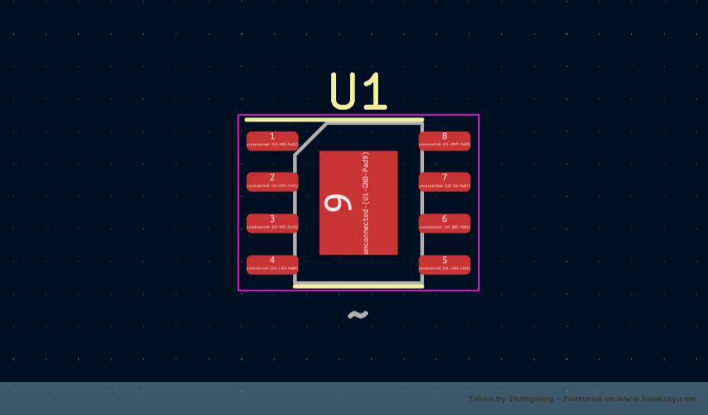
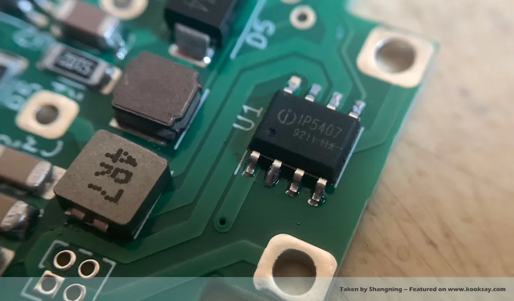
Recently, I’ve been designing and making a small circuit that uses an ESOP-8 chip. Like a standard SOP-8, it has eight pins, but it also features a thermal pad on the underside. This exposed pad serves both as a ground connection and for heat dissipation — hence the name ESOP-8, or Exposed PAD SOP-8.
While common SMD components like resistors, capacitors, and even SOP-8 chips can be hand-soldered without much trouble, the ESOP-8 package is a different case. The exposed pad makes it significantly more difficult to solder using just a soldering iron. Typically, you’d need a hot air gun or a preheater to simulate reflow soldering and get the job done properly.
Sure, hot air guns aren’t exactly rare — many electronics hobbyists have one. But even with a hot air gun, there are still some concerns: use too little solder paste, and the pad might not bond well; use too much, and you risk solder bridging between the pad and adjacent pins.
Faced with the challenge of not having a hot air gun — and the common issues even when using one — I decided to try a “lifesaver hole” as a workaround.
Experimental Pad Design: Adding a “Lifesaver Hole” to ESOP-8
For the ESOP-8 package, the most conservative footprint design looks like this: eight pins are evenly distributed on both sides, while a large rectangular exposed pad sits in the center, providing sufficient surface area for effective heat dissipation.
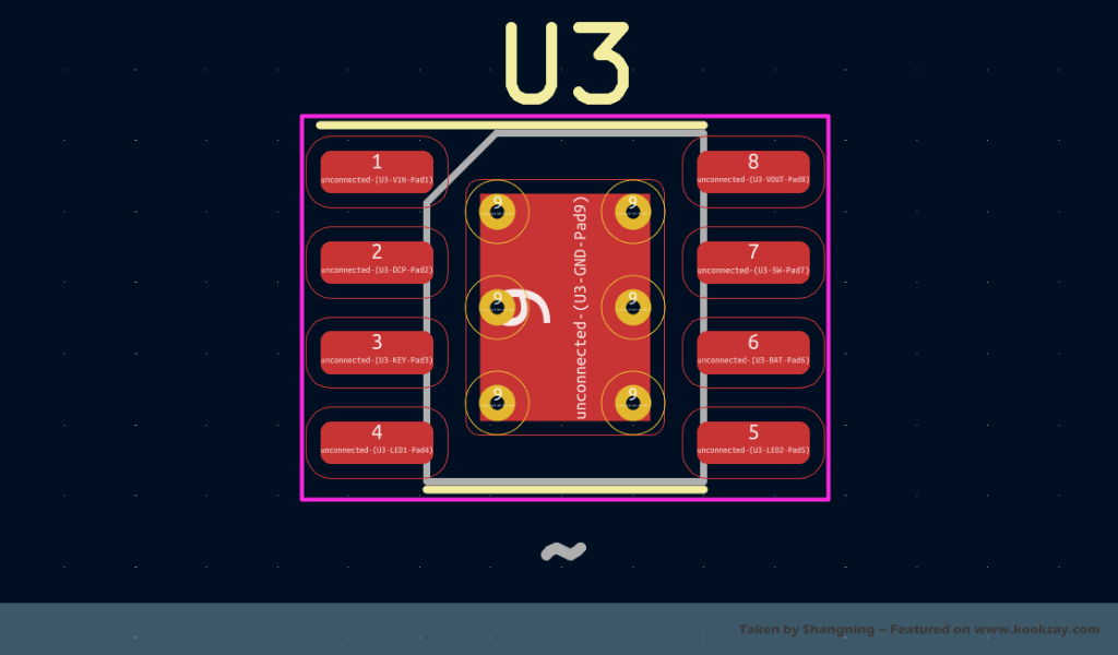
At one point, I came across an improved version of the ESOP-8 footprint that aims to enhance thermal performance further — by adding several small thermal vias (typically 0.3 to 0.4 mm in diameter) within the exposed pad area. Initially, I assumed these vias might reduce the metal contact area and introduce air pockets, which are poor thermal conductors. However, it turns out the opposite is true: these vias, when properly plated, form efficient thermal conduits that transfer heat from the chip’s exposed pad down to inner layers or the back side of the PCB, where larger copper pours help dissipate it more effectively.
Inspired by this via-enhanced design, I began experimenting with an even more aggressive idea: adding a larger plated through hole right in the center of the exposed pad. Unlike the smaller thermal vias, this hole is wide enough to allow visual inspection or even direct access during hand soldering. Effectively, it becomes a “lifesaver hole” that not only helps with thermal transfer but might also offer some practical advantages during manual assembly.
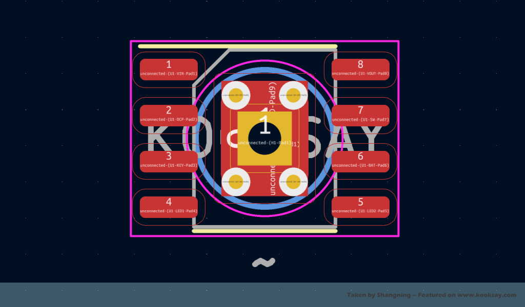
I set the diameter of the added plated through hole at 0.9 mm, which brings several potential benefits:
- The central hole isn’t large enough to introduce significant thermal resistance by way of an air gap, nor is it so small that it loses its role as a true “lifesaver” during soldering.
- After reflow or hand soldering, this hole offers a clear inspection window — ideally, you’ll see it filled with solder, not the exposed bottom of the IC.
- If you do see the bare bottom of the chip, it likely indicates a poor connection. Fortunately, the 0.9 mm diameter allows manual rework using 0.5–0.6 mm solder wire directly through the hole.
- If too much solder paste is applied during assembly, this central via acts as a natural release path, reducing the risk of solder bridging between the thermal pad and nearby pins.
While the potential benefits sound promising, they remain theoretical for now — only hands-on testing will tell whether the idea holds up in practice.
I’ve already finalized the revised pad layout with the “lifesaver hole” and generated the manufacturing files. Once the new batch of PCBs arrives, I’ll finally get to see whether this small design tweak delivers the improvements I’m hoping for.
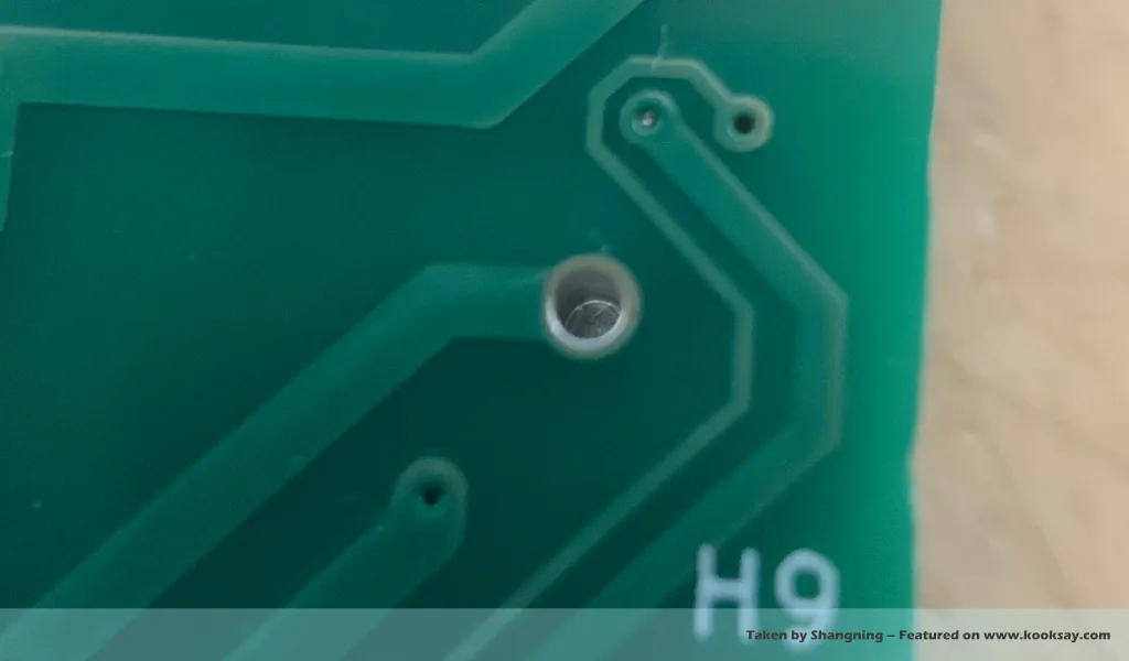
I’ve received the PCB samples, and after testing, I found that the “Lifesaver-Hole” is extremely effective for me. Now, after soldering, I can easily observe the condition of the Exposed PAD through this hole, which gives me peace of mind and makes me happy.