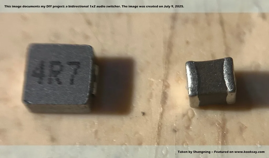
Today, I replaced the original 4x4mm surface-mount inductor I had been using with a 1210-sized surface-mount inductor. Although both inductors share the same inductance value of 4.7μH, for me, this adjustment is a necessary compromise at this stage.
The main reason for this replacement lies in the fact that the original 4x4mm inductor was extremely difficult to solder by hand. Without the aid of a hot air gun, it was nearly impossible to complete the soldering using just a soldering iron. Even though it only has two pads, both of these pads are located on the bottom of the component, making the soldering experience very similar to that of a BGA package. Even if you manage to solder one side, it’s almost impossible to find a suitable angle and space to solder the other side.
To solve this issue, I kept searching through the electronics market until I finally found an inductor with a shape very similar to a chip capacitor, using the 1210 package. This new inductor is clearly much more “hand-soldering friendly” in terms of lead design.
However, I wasn’t entirely sure whether this difference in packaging would also result in functional or performance differences. The most straightforward solution was to physically replace the component and test it. The result was reassuring: the newly selected inductor works perfectly and can fully replace the original part.
Although this problem is temporarily resolved, I still have some lingering questions in my mind: beyond the differences in packaging and appearance, is there any essential difference between these two types of inductors?
After consulting some technical resources, I learned that the inductor I had been using was a Molded Inductor, while the newly selected one is more accurately referred to as a Multilayer Chip Inductor.
In terms of performance, there are indeed significant differences between them:
Molded inductors offer higher current handling capability and excellent EMI suppression, and are widely used in power-type DC-DC converter circuits.
Multilayer chip inductors, on the other hand, have lower current capacity and average EMI performance, and are more commonly used for filtering and other signal-level applications.
In my application, the current demand is not high — only about 20mA. Therefore, at this stage, the newly selected inductor can fully meet the requirements, and so far I haven’t identified any obvious shortcomings. For me, this is an acceptable compromise. After all, the current circuit is still in the experimental stage. Once all the features are fully implemented and the product moves toward finalization, I can replace the inductor back to a more reliable molded type.
Although today’s small adjustment may seem insignificant, it has a noticeable impact on the convenience and flexibility of future development. At the same time, I feel this is also an article about hand-soldering tips, so I decided to write it down and share it here.
Please note that the solution shared here is based on my specific scenario and may not apply universally.